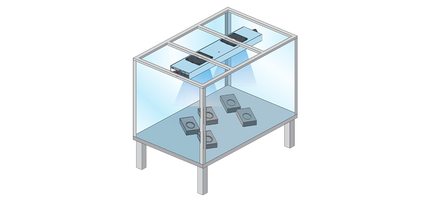
Photolithography etching static elimination
Release time:2025-08-20 Views:0
Concern
1. A batch of “dual analog switch” circuits were mounted on a PCB, and after conformal coating, a few samples showed deterioration in input characteristics.
2. After removing the aluminum, very small breakdown holes were found in the oxide layer on the n+ ring
prescription
1. After failure analysis, it was found that a short circuit and leakage occurred at the input (base) where the aluminum metallization spans the diffusion layer of the n+ protection ring.
2. Photolithographic etching is faster and electrostatic discharge damage occurs.
3. Photolithographic etching is faster and electrostatic discharge damage can occur.

Previous: Static electricity elimination inside the equipment
Next:Innovative Application Cases of Ionizer Fan in the Field of Circuit Board Anti-static
Next:Innovative Application Cases of Ionizer Fan in the Field of Circuit Board Anti-static